

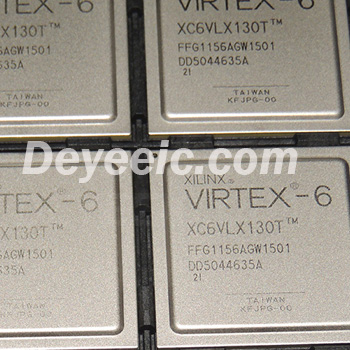
Xilinx Inc. XC6VLX130T-2FFG1156I

- Part No.:
- XC6VLX130T-2FFG1156I
- Manufacturer:
- Xilinx Inc.
- Package:
- 1156-BBGA, FCBGA
- Datasheet:
-
 XC6VLX130T-2FFG1156I.pdf
- Description:
- IC FPGA 600 I/O 1156FCBGA
- Quantity:
Unit Price:$0
Ext Price:$0
Product details
- Details
- Specifications
- FAQ
- Product Comparison
- Related Categories
The XC6VLX130T-2FFG1156I is a high-performance FPGA from Xilinx's Virtex-6 LXT family,
designed for applications demanding advanced serial connectivity and robust processing capabilities.
This technical analysis explores the chip's architectural features, performance characteristics, typical use cases,
and comparable alternatives in the FPGA market. With 128,000 logic cells, 600 I/O pins,
and support for data rates up to 6.6 Gb/s, this device offers a balanced combination of processing power and energy efficiency for complex digital systems.
The examination covers its 40nm CMOS technology, integrated PCI Express interface blocks,
and versatile configuration options that make it suitable for telecommunications, industrial automation,
and high-speed data processing applications. Additionally, the analysis provides insights into development tools
and migration paths to newer FPGA families for engineers considering design upgrades or alternatives.
Device Overview and Key Specifications
The XC6VLX130T-2FFG1156I represents a significant offering in Xilinx's Virtex-6 LXT family of field-programmable gate arrays,
delivering a robust combination of performance, flexibility, and power efficiency for demanding digital system designs.
This FPGA device stands out with its advanced feature set that addresses the needs of high-speed connectivity and signal processing applications.
Fabricated using 40nm copper CMOS process technology,
the XC6VLX130T-2FFG1156I achieves an optimal balance between performance and power consumption.
The device operates with a core voltage ranging from 0.95V to 1.05V,
with specific speed grades supporting either 1.0V standard operation or an optional low-power 0.9V mode for particularly energy-sensitive applications.
This voltage flexibility allows designers to tailor power consumption to their specific requirements without compromising functionality.
At the heart of the device's processing capability are its 128,000 logic cells organized into 10,000 configurable logic blocks (CLBs).
This substantial logic fabric provides ample resources for implementing complex digital circuits, state machines, and processing algorithms.
The CLB architecture features true 6-input lookup table (LUT) technology with dual LUT5 options,
enabling efficient implementation of wide logic functions while maintaining high utilization rates.
Each 6-input LUT can be configured as two 5-input LUTs with shared inputs, offering designers additional flexibility in resource allocation.
Memory resources in the XC6VLX130T-2FFG1156I are equally impressive, with a total of 9,732,096 RAM bits (approximately 9.28 Mbit)
distributed as both block RAM and distributed LUT RAM.
The device incorporates 36Kb block RAM/FIFO modules that can be configured as dual-port RAM (up to 36-bit wide) or simple dual-port RAM (up to 72-bit wide).
These memory blocks include enhanced programmable FIFO logic with built-in optional error correction circuitry,
particularly valuable for communication applications where data integrity is critical.
The FPGA's input/output capabilities are extensive, featuring 600 user I/O pins supporting a wide range of voltage standards from 1.2V to 2.5V.
The High-Performance Parallel SelectIO™ technology incorporates ChipSync™ for source-synchronous interfaces and
Digital Controlled Impedance (DCI) active termination, significantly simplifying board-level design while ensuring signal integrity at high speeds.
The flexible fine-grained I/O banking architecture allows mixing of different I/O standards within the same design, providing system architects with greater implementation freedom.
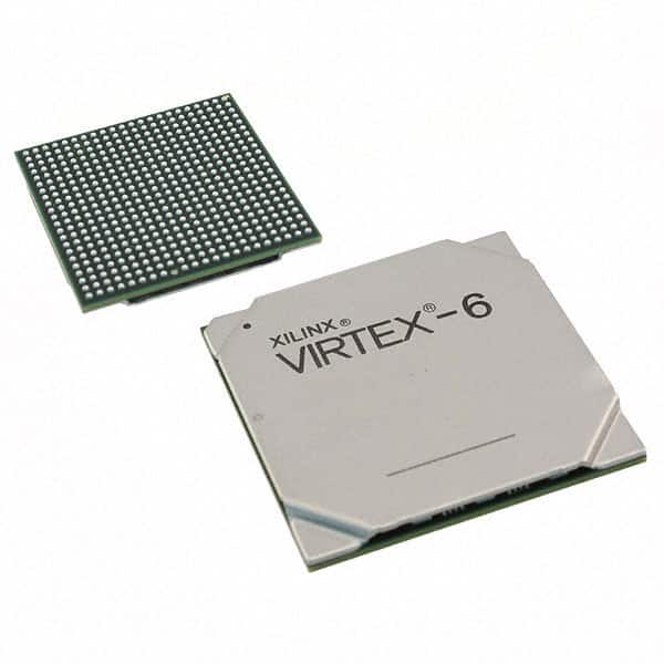
Packaged in a 1156-ball Fine-Pitch Ball Grid Array (FCBGA) measuring 35mm × 35mm,
the XC6VLX130T-2FFG1156I offers a compact footprint considering its substantial resource count.
The flip-chip packaging technology enhances signal integrity while providing effective thermal dissipation.
The device is rated for industrial temperature operation from -40°C to +100°C junction temperature,
making it suitable for deployment in challenging environmental conditions.
Key specifications of the XC6VLX130T-2FFG1156I include:
-
Logic Resources: 128,000 logic cells in 10,000 CLBs
-
Memory: 9.28 Mbit total (36Kb blocks + distributed RAM)
-
DSP Slices: Advanced DSP48E1 slices with 25×18 multipliers
-
I/O Pins: 600 user I/O supporting multiple voltage standards
-
Transceivers: 20 high-speed serial transceivers up to 6.6 Gb/s
-
Clock Management: Mixed-Mode Clock Managers (MMCM) for flexible clock generation
-
Process Technology: 40nm copper CMOS
-
Power Supply: 0.95V to 1.05V core voltage
-
Package: 1156-FCBGA (35×35mm)
-
Temperature Range: -40°C to +100°C junction temperature
The device's combination of high logic density, abundant memory, flexible I/O,
and advanced clock management positions it as a versatile solution for applications requiring substantial processing power coupled with high-speed connectivity.
Its balanced architecture makes it particularly suitable for bridging operations between processors and peripheral devices, implementing custom accelerators,
or processing high-bandwidth data streams in real-time systems.
Architectural Features and Technical Capabilities
The XC6VLX130T-2FFG1156I FPGA boasts a sophisticated architecture that combines high-performance logic fabric with specialized functional blocks,
enabling efficient implementation of complex digital systems.
This section delves into the device's internal structure and technical capabilities that distinguish it within the Virtex-6 LXT family and make it suitable for demanding applications.
Advanced Logic Fabric and Routing
At the core of the XC6VLX130T-2FFG1156I's architecture lies its highly optimized logic fabric, organized around the configurable logic block (CLB) structure.
Each CLB contains multiple slices that implement the basic logic functions.
The device utilizes a true 6-input lookup table (LUT) technology that can be configured as either a single 6-input LUT or two 5-input LUTs with common inputs.
This flexibility allows for more efficient implementation of wide logic functions while preserving resources when narrower functions are required.
The LUTs can also be configured as 64-bit (or two 32-bit) distributed RAM elements or as SRL32/dual SRL16 shift registers with registered outputs,
providing additional memory resources distributed throughout the fabric.
The routing architecture has been significantly enhanced in the Virtex-6 family compared to previous generations.
The XC6VLX130T-2FFG1156I benefits from improved routing efficiency with optimized interconnect patterns that reduce signal propagation delays and increase achievable clock frequencies.
The device features dedicated carry chains for arithmetic functions and specialized routing for wide multiplexers,
enabling efficient implementation of mathematical operations and data path elements.
With a maximum clock frequency reaching 1,286 MHz and CLB combinatorial delays as low as 4.29 ns,
the FPGA delivers performance suitable for even the most timing-critical applications.
Memory Subsystem and DSP Capabilities
The memory architecture of the XC6VLX130T-2FFG1156I is designed to support high-bandwidth data processing applications.
The device incorporates 9.28 Mbit of total RAM, organized as both block RAM and distributed LUT RAM.
The block RAM modules are configurable as 36Kb blocks that can alternatively be split into two independent 18Kb blocks, providing flexibility in memory organization.
These memory blocks support true dual-port operation with configurable width (up to 36 bits per port) and include enhanced FIFO control logic with built-in error correction capabilities,
particularly valuable for communication systems and data buffering applications.
For digital signal processing tasks, the FPGA is equipped with advanced DSP48E1 slices that provide high-performance arithmetic and logic capabilities.
Each DSP slice includes a 25×18 bit two's complement multiplier followed by a 48-bit accumulator, all with optional pipeline registers for high-throughput operation.
The DSP blocks feature new capabilities such as a pre-adder for filter applications,
bit-wise logical functions, and dedicated cascade connections that enable the construction of complex DSP datapaths without consuming general fabric resources.
These features make the XC6VLX130T-2FFG1156I particularly suitable for implementing finite impulse response (FIR) filters, fast Fourier transforms (FFTs), and other mathematically intensive algorithms.
High-Speed Serial Connectivity
One of the standout features of the XC6VLX130T-2FFG1156I is its robust high-speed serial connectivity, enabled by 20 integrated GTX transceivers capable of operating at data rates up to 6.6 Gb/s.
These transceivers support numerous industry-standard protocols including PCI Express® (as both root complex and endpoint in x1, x2, or x4 configurations),
Serial ATA (1.5/3.0/6.0 Gb/s), and DisplayPort (1.62/2.7/5.4 Gb/s).
The transceivers incorporate sophisticated clock data recovery (CDR) circuitry and equalization techniques to maintain signal integrity across various media and distances.
For PCI Express implementations, the device includes dedicated integrated interface blocks that comply with PCI Express Base Specification 2.0,
supporting both Gen1 (2.5 Gb/s) and Gen2 (5.0 Gb/s) operation.
These blocks handle the physical layer and data link layer protocol requirements, significantly reducing the FPGA fabric resources needed to implement PCIe interfaces.
Similarly, the integrated 10/100/1000 Mb/s Ethernet MAC blocks support various interface standards including 1000BASE-X PCS/PMA (via GTX transceivers)
and MII/GMII/RGMII (via SelectIO resources),
making the device well-suited for network applications.
Clock Management and System Monitoring
The XC6VLX130T-2FFG1156I features robust clock management capabilities through its Mixed-Mode Clock Managers (MMCMs)
These advanced clock generators provide zero-delay buffering, frequency synthesis, clock phase shifting, input jitter filtering,
and phase-matched clock division. The MMCMs offer finer control and better jitter performance compared to the Digital Clock Managers (DCMs)
found in earlier Xilinx families, enabling more precise clock generation and conditioning for high-speed interfaces and processing logic.
System monitoring is another critical aspect of the device's architecture. All Virtex-6 FPGAs, including the XC6VLX130T-2FFG1156I,
incorporate system monitor functionality that provides on-chip and off-chip monitoring of thermal and power supply conditions.
This feature includes JTAG-accessible monitoring of various parameters,
allowing for real-time system health assessment and potential early warning of operational issues.
The monitoring capabilities are particularly valuable in mission-critical applications where system reliability is paramount.
Configuration and Security Features
The FPGA offers flexible configuration options supporting both master and slave modes through various interfaces including SPI and parallel flash interfaces.
The device features automatic bus width detection and multi-bitstream support with dedicated fallback reconfiguration logic,
enhancing system reliability by allowing automatic recovery from configuration errors.
For secure applications, the XC6VLX130T-2FFG1156I provides several security features including bitstream encryption to
protect intellectual property and prevent unauthorized device programming.
The combination of these architectural features makes the XC6VLX130T-2FFG1156I a versatile platform for implementing complex
digital systems requiring high-performance processing, substantial memory resources, and robust connectivity options.
Its balanced mix of logic, DSP, and serial capabilities positions it as an effective solution for bridging between processing elements
and high-speed peripherals or as a standalone processing engine in data-intensive applications.
Application Domains and Implementation Scenarios
The XC6VLX130T-2FFG1156I FPGA finds extensive application across multiple industries due to its robust combination of high-speed serial connectivity,
substantial logic resources, and signal processing capabilities. This section explores the primary application domains where this FPGA excels,
highlighting implementation scenarios that leverage its unique architectural features.
Telecommunications and Networking Systems
In the telecommunications sector, the XC6VLX130T-2FFG1156I serves as a cornerstone technology for various networking equipment,
including routers, switches, and base station components.
Its integrated GTX transceivers supporting data rates up to 6.6 Gb/s make it particularly suitable for implementing high-speed serial interfaces such as 10 Gigabit Ethernet,
OTN (Optical Transport Network), and CPRI (Common Public Radio Interface) for wireless infrastructure.
The device's ability to handle multiple protocols simultaneously allows network equipment manufacturers to design versatile platforms that can be adapted to different standards and regional requirements.
The integrated 10/100/1000 Mb/s Ethernet MAC blocks significantly reduce the logic resources required to implement network interfaces,
while the support for various physical layer interfaces (including SGMII via GTX transceivers and RGMII via SelectIO resources) provides flexibility in connecting to different PHY devices.
Telecom applications particularly benefit from the FPGA's advanced clock management capabilities, which enable precise synchronization required in timing-sensitive network equipment.
The device's capacity to implement complex traffic management algorithms, packet processing engines, and quality-of-service (QoS) mechanisms in hardware makes it invaluable for building intelligent networking solutions.
Digital Signal Processing and Video Applications
The XC6VLX130T-2FFG1156I's array of DSP48E1 slices and abundant block RAM resources position it as a powerful platform for digital signal processing tasks.
In video processing applications, the FPGA can handle real-time processing of high-definition and even 4K video streams,
performing operations such as scaling, deinterlacing, color space conversion, and compression/decompression.
The parallel processing capability of the FPGA fabric allows for implementation of highly optimized video
pipelines that outperform traditional processor-based solutions in both performance and power efficiency.
Medical imaging systems leverage the device's capabilities for real-time image reconstruction in CT and MRI scanners,
where the combination of high-speed I/O and DSP resources enables processing of massive data streams from sensor arrays.
The FPGA's ability to implement custom floating-point or fixed-point arithmetic pipelines
allows medical equipment designers to optimize their algorithms for both accuracy and throughput.
Similarly, in military and aerospace applications, the device's radiation-tolerant characteristics (when appropriately mitigated)
and signal processing capabilities make it suitable for radar and sonar signal processing, where real-time performance is critical.
Industrial Automation and Control Systems
The industrial sector benefits from the XC6VLX130T-2FFG1156I's combination of reliability, performance, and interface flexibility.
In factory automation systems, the FPGA can serve as a high-performance programmable logic controller (PLC) or as a motion control coprocessor,
handling multiple axes of control with precise timing. The device's industrial temperature range (-40°C to +100°C)
ensures reliable operation in harsh factory environments where temperature extremes are common
Industrial networking applications utilize the FPGA's ability to implement various fieldbus protocols
(such as PROFINET, EtherCAT, or Powerlink) alongside custom control algorithms6. The integrated Ethernet
MAC blocks simplify the implementation of industrial Ethernet solutions, while the general-purpose logic fabric can handle protocol-specific real-time requirements.
For safety-critical applications, the FPGA's reconfigurability allows for implementation of diverse redundancy and voting schemes to meet safety integrity level (SIL) requirements.
Data Center and Computing Applications
In data center equipment, the XC6VLX130T-2FFG1156I finds use in storage controllers,
network interface cards, and computational accelerators
The integrated PCI Express interface blocks (supporting up to Gen2 x8) enable high-bandwidth connection to host systems,
while the substantial logic resources can implement custom processing pipelines for specialized workloads such as financial analytics,
database acceleration, or machine learning inference.
The FPGA's ability to handle multiple high-speed serial protocols simultaneously makes
it suitable for storage applications requiring interfaces to both host systems (PCIe) and storage media (SATA or SAS).
The device serves as an effective bridge between processors and various peripherals in heterogeneous computing systems.
Its configurable I/O supports interfacing with different memory technologies (DDR2/3, QDRII+, RLDRAM) and various processor buses,
allowing system architects to integrate components that might otherwise be incompatible.
This bridging capability is particularly valuable in legacy system upgrades where new processors need to interface with existing peripheral components.
Aerospace and Defense Systems
Military and aerospace applications leverage the XC6VLX130T-2FFG1156I for signal intelligence, electronic warfare, and secure communications systems.
The FPGA's high-speed serial transceivers are capable of handling sophisticated modulation schemes used in modern radar and communication systems,
while the logic fabric can implement complex encryption algorithms for secure data links.
The device's ability to process wideband signals in real time makes it valuable for spectrum monitoring and signal analysis applications.
In avionics systems, the FPGA serves as a reconfigurable processing platform for flight control systems, sensor fusion, and display generation.
The availability of radiation-tolerant versions (though not specifically the -2FFG1156I variant) makes
the Virtex-6 family suitable for space applications where reconfigurability in orbit provides mission flexibility and longevity. T
he device's system monitoring capabilities are particularly valuable in aerospace applications where operational integrity is critical.
Emerging Applications in AI and Edge Computing
While not specifically designed for artificial intelligence applications,
the XC6VLX130T-2FFG1156I's DSP slices and parallel processing capability make it suitable for implementing certain machine learning inference algorithms at the edge.
The FPGA can accelerate neural network layers, particularly those based on convolutional operations,
in power-constrained environments where GPUs might be impractical.
The device's ability to implement custom precision arithmetic (such as 8-bit or 4-bit integer operations) allows for optimized implementations of quantized neural networks.
In Internet of Things (IoT) gateways, the FPGA serves as a protocol bridge and preprocessing engine,
aggregating and processing data from multiple sensors before transmission to cloud services
The integrated security features, including bitstream encryption and physical protection mechanisms,
help protect intellectual property and secure device operation in potentially hostile environments.
The FPGA's low-power modes (available in certain speed grades) extend battery life in portable or remote applications.
Across these diverse application domains, the XC6VLX130T-2FFG1156I provides system architects with a balance of performance,
flexibility, and power efficiency. Its comprehensive feature set enables solutions that would otherwise require multiple discrete components,
reducing system complexity while improving reliability. The FPGA's continued availability and mature tool support make
- Package/Case:
- 1156-BBGA, FCBGA
- Packaging:
- Tray
- Series:
- Virtex®-6 LXT
- ProductStatus:
- Active
- NumberofLABs/CLBs:
- 10000
- NumberofLogicElements/Cells:
- 128000
- TotalRAMBits:
- 9732096
- NumberofI/O:
- 600
- NumberofGates:
- -
- Voltage-Supply:
- 0.95V ~ 1.05V
- MountingType:
- Surface Mount
- OperatingTemperature:
- -40°C ~ 100°C (TJ)
- Datasheet:
-
XC6VLX130T-2FFG1156I.pdf
1. How to order XC6VLX130T-2FFG1156I on Deyee Tech Limited?
Currently, Deyee Tech Limited only provide peer-to-peer order processing. While you submit the RFQ, our professional agent will contact you with the competitive prices in the global market, and our agent will prompt you to finish the order if you accept our offers.
2. How does Deyee Tech Limited guarantee that XC6VLX130T-2FFG1156I is from the original manufacturer or authorized agents?
We have a professional and experienced quality control team to strictly verify and test the XC6VLX130T-2FFG1156I. All suppliers must pass our qualification reviews before they can publish their products including XC6VLX130T-2FFG1156I on Deyee Tech Limited; we pay more attention to the channels and quality of XC6VLX130T-2FFG1156I products than any other customer. We strictly implement supplier audits, so you can purchase with confidence.
3. Are the XC6VLX130T-2FFG1156I price and inventory displayed accurate?
The price and inventory of XC6VLX130T-2FFG1156I fluctuates frequently and cannot be updated in time, it will be updated periodically within 24 hours. And, our quotation usually expires after 5 days.
4. What forms of payment are accepted?
Wire Transfer, PayPal, Alipay, Wechat, Credit Card, Western Union, MoneyGram, and Escrow are all acceptable.
Warm Tips: Some orders in certain payment forms may require handling fee.
5. How is the shipping arranged?
Customers can choose industry-leading freight companies, including DHL, UPS, FedEx, TNT, and Registered Mail. Shipping insurance is also available.
Once your order has been processed for shipment, our salesperson will send you an email advising you of the shipping status and tracking number.
Warm Tips: It may take up to 24 hours for the carriers to display tracking information. Usually, express delivery takes 3-5 days, and registered mail takes 25-60 days.
6. What is the process for return or replacement of XC6VLX130T-2FFG1156I?
All goods will implement Pre-Shipment Inspection (PSI), selected at random from all batches of your order to do a systematic inspection before arranging the shipment. If there is something wrong with the XC6VLX130T-2FFG1156I we delivered, we will accept the replacement or return of the XC6VLX130T-2FFG1156I only when all of the below conditions are fulfilled:
(1)Such as a deficiency in quantity, delivery of wrong items, and apparent external defects (breakage and rust, etc.), and we acknowledge such problems.
(2)We are informed of the defect described above within 90 days after the delivery of XC6VLX130T-2FFG1156I.
(3)The PartNo is unused and only in the original unpacked packaging.
Two processes to return the products:
(1)Inform us within 90 days
(2)Obtain Requesting Return Authorizations
7.How to contact us to get technical supports, such as XC6VLX130T-2FFG1156I pin diagram, XC6VLX130T-2FFG1156I datasheet?
If you need any after-sales service, please do not hesitate to contact us.
| Image | 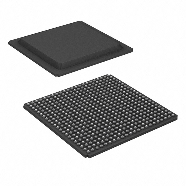 |
 |
|
|
|
| Part Number | XC6VLX75T-1FFG484C | XC6VLX75T-1FFG784C | XC6VLX75T-1FF484C | XC6VLX75T-1FF484I | XC6VLX75T-2FFG484C |
| Manufacturer | AMD Xilinx | AMD Xilinx | AMD Xilinx | AMD Xilinx | AMD Xilinx |
| Package/Case | 1156-BBGA, FCBGA | 1156-BBGA, FCBGA | 1156-BBGA, FCBGA | 1156-BBGA, FCBGA | 1156-BBGA, FCBGA |
| Packaging | Tray | Tray | Tray | Tray | Tray |
| Series | Virtex®-6 LXT | Virtex®-6 LXT | Virtex®-6 LXT | Virtex®-6 LXT | Virtex®-6 LXT |
| ProductStatus | Active | Active | Active | Active | Active |
| NumberofLABs/CLBs | 10000 | 10000 | 10000 | 10000 | 10000 |
| NumberofLogicElements/Cells | 128000 | 128000 | 128000 | 128000 | 128000 |
| TotalRAMBits | 9732096 | 9732096 | 9732096 | 9732096 | 9732096 |
| NumberofI/O | 600 | 600 | 600 | 600 | 600 |
| NumberofGates | - | - | - | - | - |
| Voltage-Supply | 0.95V ~ 1.05V | 0.95V ~ 1.05V | 0.95V ~ 1.05V | 0.95V ~ 1.05V | 0.95V ~ 1.05V |
| MountingType | Surface Mount | Surface Mount | Surface Mount | Surface Mount | Surface Mount |
| OperatingTemperature | -40°C ~ 100°C (TJ) | -40°C ~ 100°C (TJ) | -40°C ~ 100°C (TJ) | -40°C ~ 100°C (TJ) | -40°C ~ 100°C (TJ) |
- Audio Special Purpose(1538)
- Clock/Timing - Application Specific(8358)
- Clock/Timing - Clock Buffers, Drivers(4451)
- Clock/Timing - Clock Generators, PLLs, Frequency Synthesizers(31012)
- Clock/Timing - Delay Lines(1026)
- Clock/Timing - IC Batteries(4)
- Clock/Timing - Programmable Timers and Oscillators(23213)
- Clock/Timing - Real Time Clocks(2323)
- Data Acquisition - ADCs/DACs - Special Purpose(2816)
- Data Acquisition - Analog Front End (AFE)(767)
- Data Acquisition - Analog to Digital Converters (ADC)(15790)
- Data Acquisition - Digital Potentiometers(6371)
- Data Acquisition - Digital to Analog Converters (DAC)(12303)
- Data Acquisition - Touch Screen Controllers(984)
- Embedded - CPLDs (Complex Programmable Logic Devices)(5034)
- Embedded - DSP (Digital Signal Processors)(3662)
- Embedded - FPGAs (Field Programmable Gate Array)(25330)
- Embedded - FPGAs (Field Programmable Gate Array) with Microcontrollers(81)
- Embedded - Microcontrollers(90064)
- Embedded - Microcontrollers - Application Specific(2371)
XC6VLX130T-2FFG1156I Relevant information
- Popular Search
- Include Parts
The following parts are popular search parts in Embedded - FPGAs (Field Programmable Gate Array).
The following parts include "XC6VLX130T-2FFG1156I" in ISSI, Integrated Silicon Solution Inc“XC6VLX130T-2FFG1156I”.
- Part Number
- Manufacturer
- Package
- Description
In Stock:3,096
Please send RFQ..please send RFQ , we will respond immediately.


-
XCV600-5BG432I
AMD Xilinx
-
XCV600-5BG560C
AMD Xilinx
-
XCV600-5BG560I
AMD Xilinx

-
XCV600-5FG676C
AMD Xilinx
-
XCV600-5FG676I
AMD Xilinx
-
XCV600-5FG680C
AMD Xilinx
-
XCV600-5FG680I
AMD Xilinx
-
XCV600-5HQ240C
AMD Xilinx
-
XCV600-5HQ240I
AMD Xilinx
-
XCV600-6BG432C
AMD Xilinx

- Help you to save your cost and time.

- Reliable package for your goods.

- Fast reliable delivery to save time.

- Quality premium after-sale service.