

XIlinx Virtex-6 Family Overview

- Part No.:
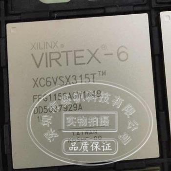
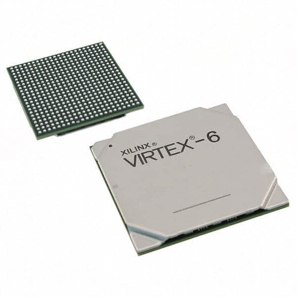
- XC6VSX315T-1FFG1156I
- Manufacturer:
- Xilinx Inc.
- Category:
- The Posts
- Package:
- 1156-BBGA, FCBGA
- Datasheet:
-
 XC6VSX315T-1FFG1156I.pdf
- Description:
- IC FPGA 600 I/O 1156FCBGA FPGA - Field Programmable Gate Array XC6VSX315T-1FFG1156I Xilinx
- Quantity:
Unit Price:$0
Ext Price:$0
Product details
- Details
- Specifications
- FAQ
- Product Comparison
- Related Categories
Virtex-6 Family Overview
General Description
Virtex®-6 FPGAs are the programmable silicon foundation for Targeted Design Platforms that deliver integrated software and hardwarecomponents to enable designers to focus on innovation as soon as their development cycle begins.
Using the third-generation ASMBL™(Advanced Silicon Modular Block) column-based architecture, the Virtex-6 family contains multiple distinct sub-families.
This overviewcovers the devices in the LXT, SXT, and HXT sub-families. Each sub-family contains a different ratio of features to most efficiently addressthe needs of a wide variety of advanced logic designs.
In addition to the high-performance logic fabric, Virtex-6 FPGAs contain many builtin system-level blocks. These features allow logic designers to build the highest levels of performance and functionality into their FPGAbased systems.
Built on a 40 nm state-of-the-art copper process technology, Virtex-6 FPGAs are a programmable alternative to customASIC technology. Virtex-6 FPGAs offer the best solution for addressing the needs of high-performance logic designers,
high-performanceDSP designers, and high-performance embedded systems designers with unprecedented logic, DSP, connectivity, and softmicroprocessor capabilities.
Summary of Virtex-6 FPGA Features
• Three sub-families:• Virtex-6 LXT FPGAs: High-performance logic withadvanced serial connectivity
• Virtex-6 SXT FPGAs: Highest signal processingcapability with advanced serial connectivity
• Virtex-6 HXT FPGAs: Highest bandwidth serialconnectivity• Compatibility across sub-families
• LXT and SXT devices are footprint compatible inthe same package• Advanced, high-performance FPGA Logic
• Real 6-input look-up table (LUT) technology• Dual LUT5 (5-input LUT) option
• LUT/dual flip-flop pair for applications requiring richregister mix• Improved routing efficiency
• 64-bit (or two 32-bit) distributed LUT RAM optionper 6-input LUT• SRL32/dual SRL16 with registered outputs option
• Powerful mixed-mode clock managers (MMCM)
• MMCM blocks provide zero-delay buffering,frequency synthesis, clock-phase shifting, inputjitter filtering, and phase-matched clock division
• 36-Kb block RAM/FIFOs• Dual-port RAM blocks• Programmable- Dual-port widths up to 36 bits- Simple dual-port widths up to 72 bits
• Enhanced programmable FIFO logic• Built-in optional error-correction circuitry• Optionally use each block as two independent18 Kb blocks
• High-performance parallel SelectIO™ technology• 1.2 to 2.5V I/O operation• Source-synchronous interfacing usingChipSync™ technology
• Digitally controlled impedance (DCI) activetermination• Flexible fine-grained I/O banking
• High-speed memory interface support withintegrated write-leveling capability
• Advanced DSP48E1 slices• 25 x 18, two's complement multiplier/accumulator• Optional pipelining
• New optional pre-adder to assist filteringapplications• Optional bitwise logic functionality
• Dedicated cascade connections• Flexible configuration options• SPI and Parallel Flash interface
• Multi-bitstream support with dedicated fallbackreconfiguration logic• Automatic bus width detection
• System Monitor capability on all devices• On-chip/off-chip thermal and supply voltagemonitoring
• JTAG access to all monitored quantities• Integrated interface blocks for PCI Express® designs
• Compliant to the PCI Express Base Specification2.0• Gen1 (2.5 Gb/s) and Gen2 (5 Gb/s) support withGTX transceivers
• Endpoint and Root Port capable• x1, x2, x4, or x8 lane support per block• GTX transceivers: up to 6.6 Gb/s
• Data rates below 480 Mb/s supported byoversampling in FPGA logic.• GTH transceivers: 2.488 Gb/s to beyond 11 Gb/s
• Integrated 10/100/1000 Mb/s Ethernet MAC block• Supports 1000BASE-X PCS/PMA and SGMIIusing GTX transceivers
• Supports MII, GMII, and RGMII using SelectIOtechnology resources• 2500Mb/s support available• 40 nm copper CMOS process technology
• 1.0V core voltage (-1, -2, -3 speed grades only)• Lower-power 0.9V core voltage option (-1L speedgrade only)
• High signal-integrity flip-chip packaging available instandard or Pb-free package options
Virtex-6 FPGA Feature Summary
XC6VLX75T
XC6VLX75T-1FF484I
XC6VLX75T-1FF784C
XC6VLX75T-1FFG484C
XC6VLX75T-1FFG484I
XC6VLX75T-1FFG784C
XC6VLX75T-1FFG784I
XC6VLX75T-2FF484I
XC6VLX75T-2FFG484C
XC6VLX75T-2FFG484I
XC6VLX75T-2FFG784C
XC6VLX75T-2FFG784I
XC6VLX75T-2FFG784C
XC6VLX75T-2FFG784I
XC6VLX75T-3FF484C
XC6VLX75T-3FFG484C
XC6VLX75T-3FFG784C
XC6VLX75T-L1FFG484C
XC6VLX130T
XC6VLX130T-1FF1156C
XC6VLX130T-1FF1156I
XC6VLX130T-1FF484I
XC6VLX130T-1FF784C
XC6VLX130T-1FFG1156C
XC6VLX130T-1FFG1156I
XC6VLX130T-1FFG484C
XC6VLX130T-1FFG484I
XC6VLX130T-1FFG784C
XC6VLX130T-1FFG784I
XC6VLX130T-2FF1156C
XC6VLX130T-2FF1156I
XC6VLX130T-2FF784I
XC6VLX130T-2FFG1156C
XC6VLX130T-2FFG1156I
XC6VLX195T
XC6VLX195T-1FF1156I
XC6VLX195T-1FFG1156C
XC6VLX195T-1FFG1156I
XC6VLX195T-1FFG784C
XC6VLX195T-1FFG784I
XC6VLX195T-2FF1156C
XC6VLX195T-2FF1156I
XC6VLX195T-2FFG1156C
XC6VLX195T-2FFG1156I
XC6VLX195T-2FFG784C
XC6VLX195T-2FFG784I
XC6VLX195T-3FF784C
XC6VLX195T-3FFG1156C
XC6VLX195T-3FFG784C
XC6VLX195T-L1FF784I
XC6VLX240T
XC6VLX240T-1FF1156I
XC6VLX240T-1FF784C
XC6VLX240T-1FF784I
XC6VLX240T-1FFG1156C
XC6VLX240T-1FFG1156I
XC6VLX240T-1FFG784C
XC6VLX240T-1FFG784I
XC6VLX240T-2FF1156I
XC6VLX240T-2FF784I
XC6VLX240T-2FFG1156C
XC6VLX240T-2FFG1156I
XC6VLX240T-2FFG784C
XC6VLX240T-3FFG1156C
XC6VLX240T-3FFG784C
XC6VLX240T-L1FF1156I
XC6VLX365T
XC6VLX365T-1FF1156I
XC6VLX365T-2FFG1156C
XC6VLX365T-2FFG1156I
XC6VLX365T-3FFG1156C
XC6VLX365T-L1FF1156I
XC6VLX550T
XC6VLX550T-1FF1759C
XC6VLX550T-1FF1760I
XC6VLX550T-1FF1759I
XC6VLX550T-1FF1760C
XC6VLX550T-2FF1759C
XC6VLX550T-2FFG1760C
XC6VLX550T-2FFG1760E
XC6VLX550T-1FFG1759C
XC6VLX550T-1FFG1759I
XC6VLX550T-L1FF1760I
XC6VLX550T-1FFG1760C
XC6VLX550T-L1FF1759C
XC6VLX550T-L1FFG1759C
XC6VLX550T-L1FFG1759I
XC6VLX550T-L1FFG1760C
XC6VLX760T
XC6VSX315T
XC6VSX315T-1FF1156I
XC6VSX315T-1FFG1156C
XC6VSX315T-1FFG1156I
XC6VSX315T-2FF1156C
XC6VSX315T-2FFG1156C
XC6VSX315T-2FFG1156I
XC6VSX475T
XC6VSX475T-1FF1156I
XC6VSX475T-1FFG1156C
XC6VSX475T-2FFG1156C
XC6VSX475T-L1FF1156I
XC6VHX250T
XC6VHX250T-1FF1154I
XC6VHX250T-1FFG1154C
XC6VHX250T-2FFG1154C
XC6VHX250T-2FFG1154I
XC6VHX250T-3FFG1154C
XC6VHX255T
XC6VHX255T-2FFG1923C
XC6VHX380T
XC6VHX380T-1FFG1924C
XC6VHX380T-2FFG1154C
XC6VHX380T-2FFG1154I
XC6VHX380T-2FFG1155C
XC6VHX380T-3FFG1155C
XC6VHX565T
XC6VHX565T-2FF1923E
XC6VHX565T-1FF1924I
XC6VHX565T-2FF1923C
XC6VHX565T-1FF1923C
XC6VHX565T-2FF1924C
XC6VHX565T-1FF1923I
XC6VHX565T-1FFG1923I
XC6VHX565T-1FFG1924C
XC6VHX565T-1FFG1924I
XC6VHX565T-2FFG1923E
XC6VHX565T-2FFG1924C
XC6VHX565T-2FFG1923C
XC6VHX565T-1FFG1923C
Notes:
1. Each Virtex-6 FPGA slice contains four LUTs and eight flip-flops, only some slices can use their LUTs as distributed RAM or SRLs.
2. Each DSP48E1 slice contains a 25 x 18 multiplier, an adder, and an accumulator.
3. Block RAMs are fundamentally 36 Kbits in size. Each block can also be used as two independent 18 Kb blocks.
4. Each CMT contains two mixed-mode clock managers (MMCM).
5. Refer to UG517, Virtex-6 FPGA Integrated Block for PCI Express User Guide for supported core pinouts by package.
6. This table lists individual Ethernet MACs per device.
7. Does not include configuration Bank 0.
8. This number does not include GTX or GTH transceivers.
Configuration
Virtex-6 FPGAs store their customized configuration in SRAM-type internal latches.
The number of configuration bits isbetween 26 Mb and 177 Mb, depending on device size but independent of the specific user-design implementation, unlesscompression mode is used.
The configuration storage is volatile and must be reloaded whenever the FPGA is powered up.
This storage can also be reloaded at any time by pulling the PROGRAM_B pin Low. Several methods and data formats forloading configuration are available, determined by the three mode pins.
Bit-serial configurations can be either master serial mode where the FPGA generates the configuration clock (CCLK) signal,or slave serial mode where the external configuration data source also clocks the FPGA.
For byte- and word-wideconfigurations, master SelectMAP mode generates the CCLK signal while slave SelectMAP mode receives the CCLK signalfor the 8-, 16-, or 32-bit-wide transfer.
Alternatively, serial-peripheral interface (SPI) and byte-peripheral interface (BPI)modes are used with industry-standard flash memories and are clocked by the CCLK output of the FPGA.
JTAG mode usesboundary-scan protocols to load bit-serial configuration data.The bitstream configuration information is generated by the ISE® software using a program called BitGen.
The configurationprocess typically executes the following sequence:
• Detects power-up (power-on reset) or PROGRAM_B when Low.
• Clears the whole configuration memory.
• Samples the mode pins to determine the configuration mode: master or slave, bit-serial or parallel, or bus width.
• Loads the configuration data starting with the bus-width detection pattern followed by a synchronization word, checksfor the proper device code, and ends with a cyclic redundancy check (CRC) of the complete bitstream.
• Start-up executes a user-defined sequence of events: releasing the internal reset (or preset) of flip-flops, optionallywaiting for the phase-locked loops (PLLs) to lock and/or the DCI to match, activating the output drivers, and transitionsthe DONE pin High.
Dynamic
Reconfiguration PortThe dynamic reconfiguration port (DRP) gives the system designer easy access to configuration bits and status registers forthree block types: 32 locations for each clock tile, 128 locations for the System Monitor,
and 128 locations for each serialGTX or GTH transceiver.The DRP behaves like memory-mapped registers, and can access and modify block-specific configuration bits as well asstatus and control registers.
Encryption, Readback, and Partial Reconfiguration
As a special option, the bitstream can be AES-encrypted to prevent unauthorized copying of the design.
The Virtex-6 FPGAperforms the decryption using the internally stored 256-bit key that can use battery backup or alternative non-volatilestorage.Most configuration data can be read back without affecting the system's operation.
Typically, configuration is an all-ornothing operation, but the Virtex-6 FPGA also supports partial reconfiguration.
When applicable in certain designs, partialreconfiguration can greatly improve the versatility of the FPGA.
It is even possible to reconfigure a portion of the FPGA whilethe rest of the logic remains active i.e., active partial reconfiguration.
CLBs, Slices, and LUTs
The look-up tables (LUTs) in Virtex-6 FPGAs can be configured as either one 6-input LUT (64-bit ROMs) with one output,
oras two 5-input LUTs (32-bit ROMs) with separate outputs but common addresses or logic inputs. Each LUT output canoptionally be registered in a flip-flop.
Four such LUTs and their eight flip-flops as well as multiplexers and arithmetic carrylogic form a slice, and two slices form a configurable logic block (CLB).
Four flip-flops per slice (one per LUT) can optionallybe configured as latches. In that case,
the remaining four flip-flops in that slice must remain unused.Between 25–50% of all slices can also use their LUTs as distributed 64-bit RAM or as 32-bit shift registers (SRL32) or as twoSRL16s.
Modern synthesis tools take advantage of these highly efficient logic, arithmetic, and memory features. Expertdesigners can also instantiate them.
- Package/Case:
- 1156-BBGA, FCBGA
- Packaging:
- Tray
- Series:
- Virtex®-6 SXT
- ProductStatus:
- Active
- NumberofLABs/CLBs:
- 24600
- NumberofLogicElements/Cells:
- 314880
- TotalRAMBits:
- 25952256
- NumberofI/O:
- 600
- NumberofGates:
- -
- Voltage-Supply:
- 0.95V ~ 1.05V
- MountingType:
- Surface Mount
- OperatingTemperature:
- -40°C ~ 100°C (TJ)
- Category:
- The Posts
- Datasheet:
-
XC6VSX315T-1FFG1156I.pdf
1. How to order XC6VSX315T-1FFG1156I on Deyee Tech Limited?
Currently, Deyee Tech Limited only provide peer-to-peer order processing. While you submit the RFQ, our professional agent will contact you with the competitive prices in the global market, and our agent will prompt you to finish the order if you accept our offers.
2. How does Deyee Tech Limited guarantee that XC6VSX315T-1FFG1156I is from the original manufacturer or authorized agents?
We have a professional and experienced quality control team to strictly verify and test the XIlinx Virtex-6 Family Overview. All suppliers must pass our qualification reviews before they can publish their products including XC6VSX315T-1FFG1156I on Deyee Tech Limited; we pay more attention to the channels and quality of XC6VSX315T-1FFG1156I products than any other customer. We strictly implement supplier audits, so you can purchase with confidence.
3. Are the XC6VSX315T-1FFG1156I price and inventory displayed accurate?
The price and inventory of XC6VSX315T-1FFG1156I fluctuates frequently and cannot be updated in time, it will be updated periodically within 24 hours. And, our quotation usually expires after 5 days.
4. What forms of payment are accepted?
Wire Transfer, PayPal, Alipay, Wechat, Credit Card, Western Union, MoneyGram, and Escrow are all acceptable.
Warm Tips: Some orders in certain payment forms may require handling fee.
5. How is the shipping arranged?
Customers can choose industry-leading freight companies, including DHL, UPS, FedEx, TNT, and Registered Mail. Shipping insurance is also available.
Once your order has been processed for shipment, our salesperson will send you an email advising you of the shipping status and tracking number.
Warm Tips: It may take up to 24 hours for the carriers to display tracking information. Usually, express delivery takes 3-5 days, and registered mail takes 25-60 days.
6. What is the process for return or replacement of XC6VSX315T-1FFG1156I?
All goods will implement Pre-Shipment Inspection (PSI), selected at random from all batches of your order to do a systematic inspection before arranging the shipment. If there is something wrong with the XC6VSX315T-1FFG1156I we delivered, we will accept the replacement or return of the XC6VSX315T-1FFG1156I only when all of the below conditions are fulfilled:
(1)Such as a deficiency in quantity, delivery of wrong items, and apparent external defects (breakage and rust, etc.), and we acknowledge such problems.
(2)We are informed of the defect described above within 90 days after the delivery of XC6VSX315T-1FFG1156I.
(3)The PartNo is unused and only in the original unpacked packaging.
Two processes to return the products:
(1)Inform us within 90 days
(2)Obtain Requesting Return Authorizations
7.How to contact us to get technical supports, such as XC6VSX315T-1FFG1156I pin diagram, XC6VSX315T-1FFG1156I datasheet?
If you need any after-sales service, please do not hesitate to contact us.
| Image |  |
 |
|
|
|
| Part Number | XC6VSX315T-1FFG1156C | XC6VSX315T-1FFG1759C | XC6VSX315T-2FFG1156C | XC6VSX315T-1FF1759C | XC6VSX315T-1FFG1156I |
| Manufacturer | AMD Xilinx | AMD Xilinx | AMD Xilinx | AMD Xilinx | Xilinx Inc. |
| Package/Case | 1156-BBGA, FCBGA | 1156-BBGA, FCBGA | 1156-BBGA, FCBGA | 1156-BBGA, FCBGA | 1156-BBGA, FCBGA |
| Packaging | Tray | Tray | Tray | Tray | Tray |
| Series | Virtex®-6 SXT | Virtex®-6 SXT | Virtex®-6 SXT | Virtex®-6 SXT | Virtex®-6 SXT |
| ProductStatus | Active | Active | Active | Active | Active |
| NumberofLABs/CLBs | 24600 | 24600 | 24600 | 24600 | 24600 |
| NumberofLogicElements/Cells | 314880 | 314880 | 314880 | 314880 | 314880 |
| TotalRAMBits | 25952256 | 25952256 | 25952256 | 25952256 | 25952256 |
| NumberofI/O | 600 | 600 | 600 | 600 | 600 |
| NumberofGates | - | - | - | - | - |
| Voltage-Supply | 0.95V ~ 1.05V | 0.95V ~ 1.05V | 0.95V ~ 1.05V | 0.95V ~ 1.05V | 0.95V ~ 1.05V |
| MountingType | Surface Mount | Surface Mount | Surface Mount | Surface Mount | Surface Mount |
| OperatingTemperature | -40°C ~ 100°C (TJ) | -40°C ~ 100°C (TJ) | -40°C ~ 100°C (TJ) | -40°C ~ 100°C (TJ) | -40°C ~ 100°C (TJ) |
- Integrated Circuits (ICs)(722936)
- RF/IF and RFID(73839)
- Discrete Semiconductor Products(253071)
- Connectors, Interconnects(1885586)
- Power Supplies - Board Mount(69900)
- Inductors, Coils, Chokes(159901)
- Isolators(22491)
- Resistors(0)
- Relays(65894)
- Capacitors(0)
- Audio Products(11654)
- Sensors, Transducers(179704)
- Circuit Protection(300347)
- Industrial Supplies(0)
- Transformers(18885)
- Tools(0)
- Test and Measurement(0)
- Tapes, Adhesives, Materials(0)
- Switches(0)
- Anti-Static Control, ESD, Clean Room Products(0)
XC6VSX315T-1FFG1156I Relevant information
- Popular Search
- Include Parts
The following parts are popular search parts in The Posts.
The following parts include "XC6VSX315T-1FFG1156I" in ISSI, Integrated Silicon Solution Inc“XIlinx Virtex-6 Family Overview”.
- Part Number
- Manufacturer
- Package
- Description
In Stock:2,094
Please send RFQ..please send RFQ , we will respond immediately.


-
XCV600-5BG432I
AMD Xilinx
-
XCV600-5BG560C
AMD Xilinx
-
XCV600-5BG560I
AMD Xilinx

-
XCV600-5FG676C
AMD Xilinx
-
XCV600-5FG676I
AMD Xilinx
-
XCV600-5FG680C
AMD Xilinx
-
XCV600-5FG680I
AMD Xilinx
-
XCV600-5HQ240C
AMD Xilinx
-
XCV600-5HQ240I
AMD Xilinx
-
XCV600-6BG432C
AMD Xilinx

- Help you to save your cost and time.

- Reliable package for your goods.

- Fast reliable delivery to save time.

- Quality premium after-sale service.